
DR Laser
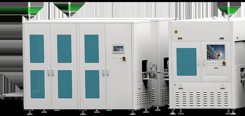
Bump PTP™ — Laser Print-Transfer-Print Metallization Line
BUMP-PTPContact for pricing
Contact Sales
Design Tools
Photonics Calculators
Explore 49 free online calculators for photonics design
Unit Converters
Convert between wavelength, frequency, power, and more
View all 49 calculators →
RoHS
REACH
DR Laser · Photovoltaic · Semiconductor · Production-scale equipment
Applications
- HJT solar cell metallization
- Micro bumping for advanced packaging (Nano Ag paste 17 μm Ø bumps; SAC305 25 μm bumps post-reflow)
- Solder paste printing; dielectric / polymer printing
Technical Notes
- Detailed line throughput, footprint and integration options available on request — please RFQ.
- Source: DR Laser Company Presentation (2026).
This is a quoted product. Pricing, lead time, and final configuration depend on substrate, throughput, and integration requirements. Use the Contact Sales button to start an RFQ — WaveQuanta acts as DR Laser's regional partner and will route your inquiry to the BD team in Singapore.
| Models | Bump PTP |
|---|---|
| Process Architecture | Laser-Induced Forward Transfer (LIFT) — Print → Fill → Laser Transfer |
| Process Steps | 1. Micro Bump pattern → 2. Solder-paste filling → 3. Laser transfer to target substrate |
| Print Materials | Nano Ag paste · SAC305 solder paste · Dielectric / polymer inks |
| Demonstrated Bump Size — Nano Ag paste | 17 μm Ø |
| Demonstrated Bump Size — SAC305 (post-reflow) | 25 μm |
| Primary Applications | HJT solar metallization · Micro bumping (advanced packaging) |
| Heritage | Built on DR Laser's PV laser-doping & laser-ablation know-how (n-IBC+HJT, TOPCON, SE-PERL, MWT-PERC, PERC heritage) |
Detailed line throughput, footprint and integration options available on request — please RFQ.
Source: DR Laser Company Presentation (2026).
Source: DR Laser manufacturer datasheet. Download the brochure (PDF) from the Documents tab for full details.
No CAD drawings available for this product.


Product Family: Industrial Laser Process Equipment (8 variants)
| Product | SKU | Size | Clear Aperture | Operating Wavelength | |
|---|---|---|---|---|---|
| Bump PTP™ — Laser Print-Transfer-Print Metallization Line Current |
BUMP-PTP
| — | — | — | |
| ThruGlas INS-510 — Panel-Level Through-Hole Inspection |
TG-INS-510
| — | — | — | Contact |
| ThruGlas CE-510 — Panel-Level Wet Etching (TGV) |
TG-CE-510
| — | — | — | Contact |
| ThruGlas LA-510 — Panel-Level Laser Modification (TGV) |
TG-LA-510
| — | — | — | Contact |
| ThruGlas INS-300 — Wafer-Level Through-Hole Inspection |
TG-INS-300
| — | — | — | Contact |
| ThruGlas CE-300 — Wafer-Level Wet Etching (TGV) |
TG-CE-300
| — | — | — | Contact |
| ThruGlas LA-300 — Wafer-Level Laser Modification (TGV) |
TG-LA-300
| — | — | — | Contact |
| Kleave Series — Laser Wafer Dicing Platform |
KLEAVE
| — | — | — | Contact |