THz Time-Domain Spectroscopy & Imaging
Two routes into the terahertz band, both supported end to end. Photoconductive-antenna TDS covers 0.1 – 5 THz with better than 75 dB dynamic range for routine spectroscopy and imaging. Organic-crystal rectification pushes past 10 MV/cm at the sample when you need to drive the material rather than probe it. WaveQuanta specifies the drive laser, emitter, relay optics, electro-optic sampling and camera as one chain.
Step 1 — Define your goal
What are you trying to achieve?
Pick the experiment / project closest to yours. We'll route you to the right system architecture and BOM.
Step 2 — Confirm the problem
Common project challenges
If any of these sound familiar, you're in the right place. WaveQuanta engineers have seen — and solved — every one of them.
The field is too weak to see a nonlinear response
Photoconductive antennas deliver V/cm to kV/cm — enough to measure a spectrum, not enough to move a material. Optical rectification in an organic crystal is the practical route to MV/cm. A fully integrated chain reaches above 10 MV/cm at a 0.14 mm focus, with 4 µJ per THz pulse from roughly 0.7 mJ of pump.
Bandwidth stops where the detection crystal stops
ZnTe rolls off near 3 THz. GaP (110) at 0.3 mm reaches roughly 0.1 – 7 THz and velocity-matches a 1030 nm Yb probe natively. Thinner crystals buy bandwidth and cost signal, so the thickness is a design decision, not a default.
Water vapour lines eat the spectrum
Rotational absorption above 0.5 THz cuts holes in the trace and inflates the apparent noise floor. A dry-purged beam path fixes it. Field numbers quoted from commissioning in open air improve once the enclosure is purged.
Scan range and frequency resolution pull against each other
600 ps of delay gives you comfortable time-domain range; extending to 3 ns is what buys sub-0.5 GHz frequency resolution. A fibre-coupled delay line reaches 50 ns of range at 5 fs resolution when you need both.
The pump laser does not match the emitter
BNA and GaP want Yb at 1030 nm. DSTMS, DAST and OH1 want roughly 1.3 – 1.5 µm, which means an OPA in front of them. Settling this before you buy the crystal avoids the most expensive mistake in a THz build.
Dynamic range is paid for in averaging time
A portable photoconductive spectrometer gives better than 75 dB as standard and better than 100 dB with options; better than 60 dB is reachable in under 10 seconds. Knowing which number your measurement actually needs decides the configuration.
The THz beam is invisible, so alignment is guesswork
TPX transmits in the visible and lets you align with a diode; silicon does not. A real-time camera or a pyroelectric power sensor turns alignment from iteration into a picture you can look at.
Organic emitter crystals are fragile and humidity sensitive
BNA and the stilbazolium salts degrade in ambient humidity and damage above a pump fluence that is rarely quoted. Dry-purged storage and an agreed fluence budget are part of the system design, not an afterthought.
Step 3 — Understand the system
Typical system architecture
Six stages, from pump to data. The bench shown is a real WaveQuanta layout, not a schematic — HELIOS-HP drive laser, HYPERION-S compressor, BNA generation, off-axis parabolic relay, and GaP electro-optic sampling read out through a Wollaston prism, balanced photodetector and lock-in. Every part on it is a catalogue item. Which stages you need, and how hard each has to work, follows from the field strength and bandwidth you are after.
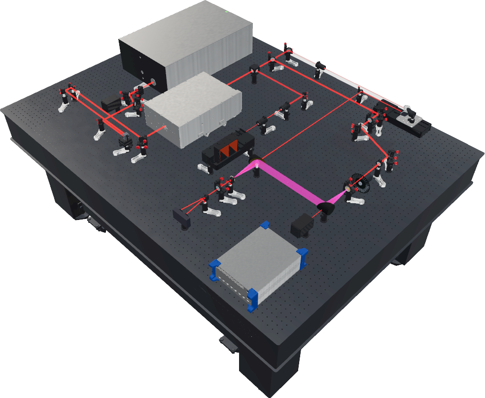
Yb at 1030 nm for BNA and GaP; Er at 1550 nm for fibre-coupled antenna stations; an OPA at 1.3 – 1.5 µm for DSTMS, DAST and OH1. Intense-field work starts around 0.7 mJ per pulse at 10 – 100 kHz, M² < 1.2, better than 0.5 % RMS over 24 h.
A gas-filled multi-pass cell takes 150 fs – 1 ps down to under 35 fs at better than 90 % efficiency, with a 5 – 10 compression ratio. A shorter pump pulse is the cheapest available bandwidth in the whole chain. A hollow-core stage can be cascaded for few-cycle output.
Photoconductive antenna under a modulated 100 V bias with sub-50 ns edges for routine TDS; optical rectification in BNA (0.5 – 3 THz, 17 mm clear aperture on sapphire), DSTMS (0.3 – 15 THz) or DAST (0.1 – 17 THz) when peak field is the objective.
90° off-axis parabolic mirrors in protected gold, better than 93 % from 2 to 30 µm, λ/8 RMS figure. Through-hole variants let the optical probe ride collinearly with the THz beam. TPX and HDPE lenses, silicon and TPX windows for cryostats and purge boxes.
Detection crystal, quarter-wave plate, Wollaston prism, balanced photodetector. Electro-optic sampling measures the field rather than the power, so amplitude and phase come out of a single scan and the complex response follows without a Kramers-Kronig step.
Lock-in referenced to an optical chopper or to the antenna bias, DC – 1 MHz with input noise below 2.4 nV/√Hz. For imaging, an uncooled microbolometer array at 160 × 120 and 25 µm pitch runs at 10 / 30 / 60 Hz with an f/0.7 objective.
Step 4 — Pick the modules
Recommended system modules
Eight building blocks, in the order the light passes through them. Each one is a category in the WaveQuanta terahertz catalogue.
fs Drive Laser and Compression
The pump decides everything downstream: emitter choice, achievable field and usable bandwidth.
- Yb 1030 nm, 10 – 20 W, up to 1 – 2 mJ per pulse
- 10 – 100 kHz, < 250 fs, M² < 1.2
- Multi-pass-cell compression to < 35 fs at > 90 %
- Er 1550 nm fibre for antenna-based stations
Pump Conditioning to 1.3 – 1.5 µm
Stilbazolium and OH1 crystals are phase-matched in the telecom band, not at 1030 nm. This stage is what makes them usable.
- OPA / OPCPA output at 1.3 – 1.5 µm
- Required for DSTMS, DAST and OH1
- Not required for BNA or GaP at 1030 nm
- Pulse diagnostics to confirm the compressed pulse
THz Emitters
Antenna for convenience and repeatability, organic crystal for field strength. The two are not interchangeable.
- BNA, CA 17 mm on 1" sapphire, 0.5 – 3 THz
- DSTMS 0.3 – 15 THz, apertures to 65 mm
- DAST 0.1 – 17 THz, higher damage threshold
- Photoconductive antennas with 100 V modulated bias
THz Relay and Beam Handling
Everything between the emitter and the sample, where most of the signal is normally lost.
- 90° OAP, 50.8 mm, RFL 152.4 mm, protected gold
- Through-hole OAPs for collinear optical probing
- TPX and HDPE lenses, near-zero THz dispersion
- Bandpass, bandstop, low- and high-pass filters to 150 mm
Sample Environment and Windows
Cryostats, vacuum chambers and purge boxes all need windows that are transparent where your measurement lives.
- High-resistivity silicon, n ≈ 3.42, flat across the band
- TPX, n ≈ 1.46, transparent in the visible
- Rigid silicon for vacuum and cryostat windows
- Dry-purged enclosures to suppress water lines
Time Base, Delay and Modulation
The time axis is the measurement. Its range sets your frequency resolution and its step size sets your bandwidth.
- Motorised delay, finest step 0.015 ps
- Fibre-coupled delay line, 50 ns range at 5 fs resolution
- Optical chopper 5 Hz – 3 kHz, TTL lock-in reference
- High-voltage antenna modulator, 100 Hz – 1 MHz
Electro-Optic Sampling Detection
Field-resolved detection: crystal, quarter-wave plate, Wollaston prism, balanced photodetector.
- GaP (110), 0.3 mm, ≈ 0.1 – 7 THz at 1030 nm
- Mounted ZnTe crystals, thickness traded against bandwidth
- Wollaston prisms and balanced InGaAs / Si detectors
- Amplitude and phase from one scan
Acquisition, Imaging and Power Metrology
Turning the detected field into data you can publish, and checking the source is doing what you think it is.
- Digital lock-in, DC – 1 MHz, < 2.4 nV/√Hz, 100 MSa/s
- Microbolometer cameras, 160 × 120, < 1 to 18 THz
- f/0.7 THz imaging objective, 0.1 – 30 THz
- Pyroelectric power sensor, NEP < 1 nW/√Hz
Step 5 — Match the configuration to the physics
Choose your configuration
The same catalogue, in three shapes. Which one you need is decided by field strength and by how much of the bench you want to build yourself.
Component Bench
Building your own TDS on a breadboard
You have a femtosecond laser and want to build the THz chain yourself. We supply the emitter, the relay optics, the detection crystal and the acquisition, matched to the pump you already own.
- BNA or GaP emitter matched to a 1030 nm pump
- 90° off-axis parabolic relay, protected gold
- GaP (110) EOS crystal, Wollaston, balanced detector
- Optical chopper and digital lock-in
- TPX / silicon windows for your sample environment
BOM tier: Quoted per BOM
Turnkey TDS and Imaging
Spectroscopy and inspection without a build phase
A fibre-coupled photoconductive spectrometer that arrives aligned. Transmission, reflection, dual-transmission and dual-reflection geometries, with a real-time camera option for imaging.
- > 5 THz standard, > 6 THz with options
- > 75 dB dynamic range, > 100 dB with options
- 600 ps scan range, 3 ns option for < 0.5 GHz resolution
- Better than 60 dB in under 10 seconds
- Optional RIGI microbolometer camera and objective
BOM tier: Configured · request quote
Intense-Field THz
Nonlinear THz driving and THz-pump experiments
The full chain, integrated and commissioned: ytterbium drive laser, multi-pass-cell compression, organic-crystal generation, a dry-purged off-axis parabolic relay and field-calibrated electro-optic sampling.
- > 10 MV/cm peak field, guaranteed floor 8 MV/cm
- 1.0 – 4.6 THz within 10 dB, usable out to 12 THz
- 4 µJ per THz pulse, 0.6 – 0.9 % conversion
- Two focus stations, 0.14 mm and 0.26 mm
- Four pump-probe configurations without rebuilding
- Factory FAT plus on-site commissioning, 24-month warranty
BOM tier: Configured · request quote
Step 6 — Run the numbers
Recommended calculators
Sanity-check your design before talking to an engineer.
Step 7 — Configure the system
Configure your setup with our engineering tools
Two ways to go from “this is what I want to do” to “this is the BOM I need”.
Open the THz Virtual Lab
Place the drive laser, compressor, generation crystal, off-axis parabolic relay, delay stage and electro-optic sampling arm on a 3D breadboard. Check beam heights and path lengths, then export the layout as a bill of materials built from real WaveQuanta part numbers.
Launch Virtual LabAsk AI to scope my THz system
Describe your sample, the spectral coverage you need and the field strength you are aiming for. The AI Concierge proposes a laser, emitter, detection scheme and imaging option in about 30 seconds.
Open AI ConciergeStep 8 — Anchor SKUs
Featured products for this application
Common picks for this application area. Your final BOM will pull from a wider catalog and be sized to your project tier.

WaveQuanta
Intense THz Spectroscopy System, Turnkey, > 10 MV/cm Peak Field

Swiss Terahertz
PCA Scanner THz Imaging Spectrometer, Portable, > 5 THz

WaveQuanta
BNA Organic THz Generation Crystal, CA 17 mm on 1" Sapphire

Swiss Terahertz
DSTMS Organic THz Generation Crystal

WaveQuanta
GaP (110) Electro-Optic Sampling Crystal, 10 x 10 x 0.3 mm

Swiss Terahertz
RIGI S2X THz Camera

WaveQuanta
90 deg Off-Axis Parabolic Mirror, Through Hole Parallel to the Collimated Beam, 2", RFL 152.4 mm, Protected Gold

Swiss Terahertz
Uri THz Power Sensor, Pyroelectric, < 1 nW/sqrt(Hz)
Step 9 — Common questions
Frequently asked questions
Quick answers to the questions our application engineers hear most often.
Photoconductive antenna or organic crystal — which emitter do I need?
The question is field strength, not preference. A photoconductive antenna is fibre-friendly, repeatable and gives better than 75 dB of dynamic range out to about 5 THz — the right answer for spectroscopy, imaging and inspection. An organic crystal under optical rectification is what you use when the measurement itself depends on field strength: BNA at 0.5 – 3 THz pumped at 1030 nm, DSTMS at 0.3 – 15 THz and DAST at 0.1 – 17 THz pumped at 1.3 – 1.5 µm. A fully integrated chain reaches above 10 MV/cm at the focus.
How much peak field can I actually expect at the sample?
On a commissioned turnkey system: above 10 MV/cm in everyday operation with a guaranteed floor of 8 MV/cm, at a 0.14 mm focus, from roughly 0.7 mJ of pump at 0.6 – 0.9 % conversion — about 4 µJ per THz pulse. Those numbers come from commissioning measurements with the beam path in open air; purging improves them. Field is calibrated by Kerr rotation in diamond and cross-checked against an independent source to within about 8 %. Published work with DSTMS pumped by a 34 mJ OPA has reached 85 MV/cm, so the ceiling is set by your pump, not the crystal.
Which detection crystal, and how thick?
GaP (110) at 0.3 mm is the default for a 1030 nm Yb probe — its optical and THz indices nearly match at 1 µm, giving roughly 0.1 – 7 THz. ZnTe is more sensitive but rolls off near 3 THz. Thickness is a direct trade: 0.1 – 0.3 mm for detection bandwidth, 0.3 – 1 mm when you want signal. In every case the detection arm is crystal → quarter-wave plate → Wollaston prism → balanced photodetector.
Why electro-optic sampling instead of a power detector?
Because EOS measures the field, not the power. You get amplitude and phase from one time-domain scan, which means the complex refractive index follows directly without a Kramers-Kronig inversion. A pyroelectric sensor measures total incident power incoherently — useful for alignment, calibration and daily power checks at below 1 nW/√Hz noise-equivalent power, but it cannot give you a spectrum.
What scan range do I need for my frequency resolution?
Frequency resolution is roughly the inverse of your delay range. 600 ps is the standard configuration; extending to 3 ns is what buys better than 0.5 GHz. If you need both long range and fine steps, a fibre-coupled optical delay line covers up to 50 ns at 5 fs resolution. On an intense-field bench the motorised stage steps down to 0.015 ps with about 1 ps time resolution.
Can I do real-time THz imaging, and at what resolution?
Yes, with an uncooled microbolometer array — no cryogens. A 160 × 120 array at 25 µm pitch covers below 1 THz to 18 THz at 10, 30 or 60 Hz over USB 3.0. Paired with an f/0.7 objective covering 0.1 – 30 THz, 3 mm features have been resolved in a single short exposure without correction. For quantitative imaging you can also raster a photoconductive spectrometer, which trades speed for spectral information per pixel.
Do I need a purge or vacuum enclosure?
Above roughly 0.5 THz, water vapour rotational lines cut visible holes in the spectrum. For survey work in a dry room you can live with it; for quantitative absorption measurements you cannot. Dry nitrogen purge is the usual answer. If your sample sits in a cryostat, high-resistivity silicon (n ≈ 3.42, nearly flat across the band, rigid enough for vacuum) or TPX (n ≈ 1.46, near-zero dispersion, transparent in the visible so you can align through it) are the two window materials to choose between.
How fragile are the organic crystals?
Handle them as consumables with a defined operating envelope. BNA and the stilbazolium salts (DSTMS, DAST) are humidity and damage sensitive and want dry-purged storage. Damage threshold differs between them — DAST tolerates more than DSTMS — so the pump fluence budget is part of the system design. Apertures up to 65 mm are available, and larger apertures let you spread the same pulse energy over more area, which is often the cheapest way to stay under threshold.
Step 10 — Engineering Review
Application Engineering Review
Tell us your application, current setup, and project context. A WaveQuanta application engineer will return initial recommendations within 1 business day.
- 1 Application
- 2 Current setup
- 3 Project & purchase