WaveQuanta
DField-VS-A4 TE-Cooled Spectroscopy CCD, -60 °C Cooling, 30.7 mm Wide Sensor
DField-VS-A4Contact for pricing
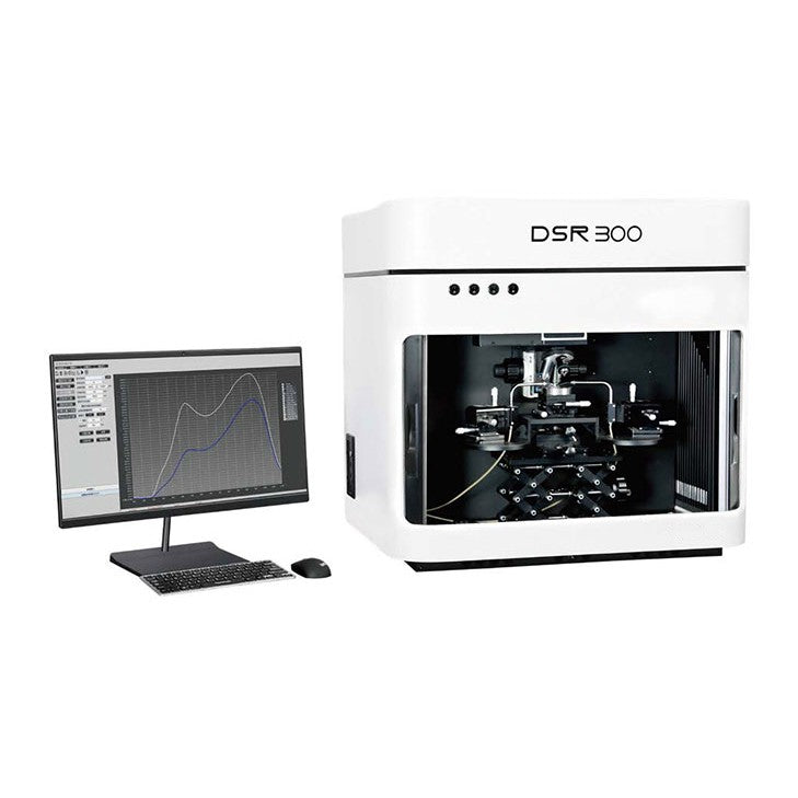
Spectral response and photocurrent mapping of micro- and nano-scale devices and low-dimensional materials.
The DSR300 series is designed for low-dimensional materials and micro-nano devices, combining spectral scanning with photocurrent scanning under a microscope. A 40 µm probe spot allows samples as small as 100 µm to be measured, and xenon, supercontinuum, CW laser and picosecond pulsed laser sources can be integrated to test different detector types. The instruments are operated automatically from the control software.
Browse all: Photoelectric Test Systems · Spectroscopic Instruments
Model: DSR300 Series · Contact WaveQuanta for a quote, configuration advice and lead time.
| Detection Spot | 40 µm (550 nm, 50× objective, 200 µm fiber) |
| Other Spot Sizes | 70 µm (400 µm fiber); 5 µm (375 nm ps laser, 40×); 80 µm (40× reflective objective) |
| Minimum Sample Size | 100 µm |
| Light Paths | 4 (3 built-in, 1 external for tunable broadband monochromatic light) |
| Xenon Light Source | 250–1800 nm, instability < 1% |
| Supercontinuum Source | 400–2400 nm, 0.01–200 MHz, 100 ps pulse width |
| CW Laser Options | 405, 532, 633, 808 or 980 nm; instability < 1% |
| Pulsed Laser Options | 375, 405, 488, 785 or 976 nm; 100 ps pulse width; 1–20 MHz |
| Objective 10× (Standard) | WD > 17 mm, NA 0.42, 350–800 nm |
| Objective 50× | WD > 17 mm, NA 0.42, 480–1800 nm |
| Objective 50× UV | WD > 12 mm, NA 0.42, 240–500 nm |
| Objective 40× Reflective | WD > 7.8 mm, NA 0.5, 200 nm–20 µm |
| Lock-in Amplifier | 20 Hz–1 kHz, 1 nV–1 V full-scale sensitivity, dynamic reserve > 100 dB |
| Lock-in Details | Voltage or current input, current gain 10⁶ or 10⁸ V/A, drift < 0.1°/°C, X/Y/R/θ display |
| Keithley 2612B | Current range 100 nA / 1 A, min. signal 1 nA, noise 100 pA, resolution 100 fA, 2 channels |
| Keithley 2636B | Current range 1 nA / 1 A, min. signal 10 pA, noise 1 pA, resolution 10 fA, 2 channels |
| Cryostat Temperature | −196 to 600 °C, resolution 0.1 °C |
| Cryostat Optics | Clear aperture 24 mm, sample area Φ22 mm, working distance 4.5–12.5 mm |
| Cryostat Chamber | Air-tight, can be filled with protective gas, independent temperature control |
| Probe Holders | 4, with 20 or 10 µm tips; XYZ adjustable, 12 mm travel, 0.75 µm resolution |
| Cabling | 2 m triaxial cable, leakage current < 1 pA |
| Sample Stage | Vacuum adsorption |
| LBIC Mapping Stage | XY travel 50 mm, resolution 5 µm, scanning spatial resolution 1 µm |
| Product | SKU | Size | Clear Aperture | Operating Wavelength | |
|---|---|---|---|---|---|
| DSR900 Camera Characteristics Measurement System, EMVA 1288, 200–2500 nm |
DSR900
| — | — | — | Contact |
| DSR500-LBIC Micro-Nano Photoelectric Imaging System, Galvo Scanning, 2 µm Spot |
DSR500-LBIC
| — | — | — | Contact |
| DSR600 Photodetector Spectral Response System, 200–2400 nm, Lock-in Detection |
DSR600 Series
| — | — | — | Contact |
| DSR300 Micro-Nano Device Spectral Response System, 40 µm Spot, LBIC Mapping Current |
DSR300 Series
| — | — | — | |
| QE-B1 Calibrated Silicon Reference Cell, 20 × 20 mm, NIST-Traceable |
QE-B1
| — | — | — | Contact |
| SCS600 Series Solar Cell Quantum Efficiency System, EQE/IQE, 300–2500 nm |
SCS600 Series
| — | — | — | Contact |
| SCS600-MAX Large-Area Solar Cell QE System, 250 × 250 mm, QE and LBIC Mapping |
SCS600-MAX
| — | — | — | Contact |
| SolarIV Series Solar Cell I-V Test System, Class A AM1.5G Simulator |
SolarIV Series
| — | — | — | Contact |
| Sirius Series Solar Simulators, Class A AM1.5G, 0.2–1.2 Sun Adjustable |
Sirius Series
| — | — | — | Contact |